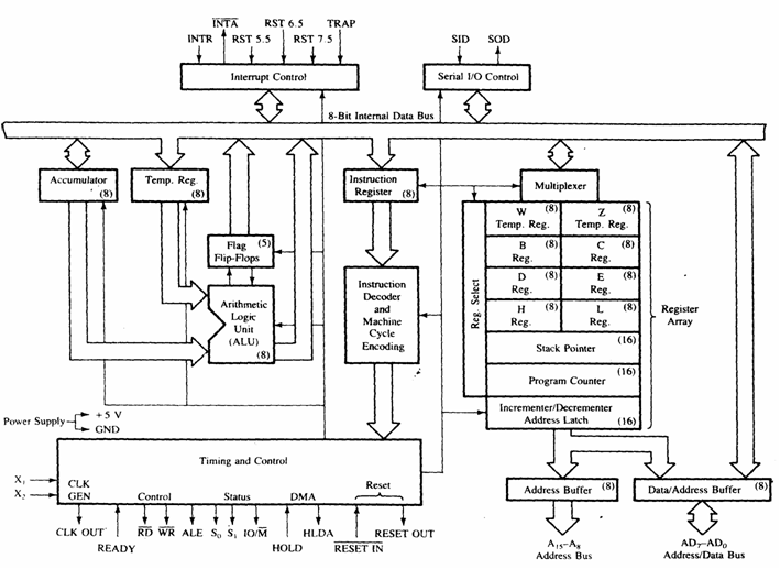
Internal Architecture and Features of 8085
Internal Architecture of 8085 Microprocessor
1. ALU:
- It performs arithmetic and logic functions.
- It includes accumulator, temp register, arithmetic and logic circuits and five flags.
- Temp register holds the data during arithmetic and logic operation.
- Accumulator stores the result.
- Flags are set/reset based on operation.
- Flags are generally a flip flop.
- The flags are:
| S | Z | - | AC | - | P | - | CY |
2. Registers:
- IR receives opcode of instruction from data bus and passes to decoder.
- Register array (B, C, D, E) is a 8 bit register accessible to programmers where data can be stored during program execution.
- H and L registers can also be used by the programmers.
- SP points to memory location in R/W memory.
- PC is used to sequence the execution of instructions.
3. Timing and Control:
- It is responsible for synchronizing all operation with clock.
- It generates the control signals.
4. Interrupt Control:
- It is used to interrupt a microprocessor.
5. Serial I/O Control:
- It is used for serial data transmission.
Features of 8085 Microprocessor
The basic features of 8085 microprocessor are as follows:
a) 8-bit microprocessor
b) It can address 64K of memory.
c) It is supplied with 40 pins.
d) It requires +5 V single power supply.
e) It can operate with 3-MHz single phase clock.
Instruction Format and Data Format of 8085
Instruction Format
- Instruction is a command given to the microprocessor to perform some specific task.
- Based on word size, instruction set is classified into 1-byte, 2-byte and 3-byte instructions.
a) 1-byte Instruction:
- It includes the opcode and the operand in the same byte.
- These instructions are stored in 8 bit binary format in memory.
- Eg: MOV C, A ; ADD B ; CMA
b) 2-byte Instruction:
- It includes opcode in first byte and operand in second byte.
- They are stored in two memory locations.
- Eg: MVI A, 32H
c) 3-byte Instruction:
- It includes opcode in first byte and the remaining two bytes specify 16-bit address.
- The second byte includes low-order address.
- The third byte includes high-order address.
- Eg: LDA 2050H ; JMP 2085H
Data Format
- Data are represented in the form of ASCII code, BCD code, signed integer and unsigned integer.
Addressing Modes of 8085
- The way of specifying data in an instruction is known as addressing modes.
- The common addressing modes used by 8085 microprocessors are as follows:
1. Direct Addressing:
- Data is directly copied from given address to the register.
- Eg: LDA 3000H (Content of location 3000H is copied to accumulator)
IN 00H (Read data from port 00H)
2. Immediate Addressing:
- Data is transferred directly to the register.
- Eg: MOV A, 30H (Data 30H is copied to register A)
3. Register Addressing:
- Data is copied from one register to another.
- Eg: MOV A, B (Content of B is copied to register A)
4. Indirect Addressing:
- Data is transferred from address pointed by the content of register into another register.
- Eg: MOV A, M (Data pointed by the content of memory location is transferred to A)
5. Implied Addressing:
- Data is specified by opcode itself.
- It does not need any operand.
Instruction Sets of 8085
Data Transfer:
MVI R, 8 bit //Load 8 bit data in a register R
MOV Rd, Rs //Copy data from source register Rs to destination register Rd
LXI Rp, 16 bit // Load 16 bit data in a register pair Rp
OUT 8 bit // Send data byte from accumulator to output device
IN 8 bit // Accept data byte from input device and put it to accumulator
LDA 16 bit // Copy data byte from 16 bit address to accumulator
STA 16 bit // Copy data byte from A into 16 bit address memory
LDAX Rp // Load to A from memory specified by Rp
STAX Rp // Store to memory specified by Rp with data from A
MOV R, M //Copy data into register from memory
MOV M, R //Copy data into memory from register
Arithmetic and Logical Instructions:
ADD R/M //Add the content of specified register or memory with accumulator
ADI 8 bit // Add the 8 bit data with accumulator
SUB R/M // Subtract the content of specified register or memory from accumulator
SUI 8 bit //Subtract 8 bit data from accumulator
INR R/M //Increment the value of register or memory
DCR R/M //Decrement the value of register or memory
INX Rp //Increment values of register pair Rp
DCX Rp //Decrement values of register pair Rp
ANA R/M // Logical AND with accumulator
ANI 8 bit // Logical AND with accumulator
ORA R/M // Logical OR with accumulator
ORA 8 bit // Logical OR with accumulator
XRA R/M // Logical XOR with accumulator
XRI 8 bit // Logical XOR with accumulator
CMP R //Complement
CPI 8 bit //Complement
Branch Instructions:
JMP 16-bit address //Jump to specified address
JZ 16-bit address //Jump to specified address if zero flag set
JNZ 16-bit address //Jump to specified address if zero flag reset
JC 16-bit address //Jump to specified address if carry flag set
JNC 16-bit address //Jump to specified address if carry flag reset
CALL 16-bit address //Call location of a subroutine
RET //Return to a calling program
Various Example Programs
1. WAP to add upper and lower nibble of ten 8 bit words stored in a table that starts from 8B20H. Store separate results in locations just after the table.
LXI H, 8B20H
LXI D, 8B30H
MVI B, OAH
L1: MOV A, M
ANI OFH
MOV B, A
MOV A, M
ANI FOH
RRC
RRC
RRC
RRC
ADD B
MOV D, A
INX H
INX D
DCR B
JNZ L1
HLT
2. WAP such that table 1 contains 16 no of 8 bit data, transfer data which have no of 1’s greater than 3 from table 1 to table 2, otherwise store FFH in table 2.
LXI H, 8000H ; TABLE 1
LXI D, 9000H ; TABLE 2
L1: MVI B, 08H ; COUNT OF NO OF BITS
MVI C, 00H ; COUNT OF NO OF 1’S
MOV A, M
L2: RLC
JNC L3
INR C
L3: DCR B
JNZ L2
MOV A, C
CPI 03H
MOV A, FFH
JC L4
JZ L4
MOV A, M
L4: STAX D
INX H
INX D
MOV A, E
CPI 10H
JNZ L1
HLT
3. WAP to exchange bits D6 and D2 of every byte. Suppose there are 200 bytes in the program starting from memory location 8090H.
LXI H, 8090H
MVI B, C8H
L1: MOV A, M
ANI 44H
MVI C, 08H
MVI D, 00H
L2: RLC
JNC L3
INR D
L3: DCR C
JNZ L2
MOV A, D
CPI 01H
MOV A, M
JNZ L4
XRI 44H
L4: MOV M, A
INX H
DCR B
JNZ L1
HLT
4. WAP to divide a byte stored in location 9070H by byte stored in 9071H and store remainder and quotient at 9072H and 9073H respectively.
LXI H, 9070H
MOV A, M
LXI H, 9071H
MOV B, M
MVI C, 00H
L2: CMP B
JC L1
SUB B
INR C
JMP L2
L1: STA 9072H
MOV A, C
STA 9073H
HLT
5. WAP to convert ten BCD numbers at 4350H to binary and store at 4360H.
LXI SP, Stack
LXI H, 4350H
LXI B, 4360H
MVI D, 0AH
L1: MOV A, M
CALL BCDTOBIN
STAX B
INX H
INX B
DCR D
JNZ L1
HTL
BCDTOBIN: PUSH B
PUSH D
MOV B, A
ANI 0FH
MOV C, A
MOV A, B
ANI F0H
JZ BCD1
RRC
RRC
RRC
RRC
MOV D, A
XRA A
MVI E, 0AH
SUM: ADD E
DCR D
JNZ SUM
BCD1: ADD C
POP D
POP B
RET
6. WAP to transfer bytes of data with odd parity from 9205H to A200H, else transfer by clearing bit D5 and setting bit D3. The end of bytes is indicated by 51H in the data.
LXI H, 9205H
LXI B, A200H
L1: MOV A, M
JPO L2
ANI DFH
ORI 08H
L2: STAX B
MOV A, M
INX H
INX B
CPI 51H
JNZ L1
HLT
7. WAP to transfer 8-bit number from one table to other by setting bit D5 if no is less than 80H else transfer by resetting bit D6.
LXI H, 8000H ; SOURCE TABLE
LXI D, 9000H ; DESTINATION TABLE
MVI B, 0AH ; CONSIDER 10 8-BIT NUMBERS
L1: MOV A, M
CPI 80H
JC L2
ANI BFH
JMP L3
L2: ORI 20H
L3: STAX D
INX H
INX D
DCR B
JNZ L1
HLT
8. WAP to load memory locations 7090H and 7080H with data 40H and 50H and then swap these data.
MVI H, 70H
MVI L, 90H
MVI A, 40H
MOV M, A
MOV C, M
MVI L, 80H
MVI B, 50H
MOV M, B
MOV D, M
MOV M, C
MVI L, 90H
MOV M, D
HLT
9. WAP to add two 4 digit BCD numbers equals 7342 and 1989 and store result in BC register.
LXI H, 7342H
LXI B, 1989H
MOV A, L
ADD C
DAA
MOV C, A
MOV A, H
ADC B
DAA
MOV B, A
HLT
10. WAP to add 16 bit numbers in register BC (2793H) and register DE (3182H) and place sum in memory locations 2050H and 2051H.
MOV A, C
ADD E
MOV L, A
MOV A, B
ADC D
MOV H, A
SHLD 2050H
HLT
11. WAP to move 10 bytes of data from starting address 9500H to 9600H.
MVI B, 0AH
LXI H, 9500H
LXI D, 9600H
L1: MOV A, M
STAX D
INX H
INX D
DCR B
JNZ J1
HLT
12. WAP to transfer 30 data starting from 8500 to 9500H if data is odd else store 00H.
MVI B, 1EH
LXI H, 8500H
LXI D, 9500H
L2: MOV A, M
ANI 01H
JNZ L1
MVI A, 00H
JMP L3
L1: MOV A, M
L3: STAX D
INX H
INX D
DCR B
JNZ L2
HLT
13. WAP to sort in ascending order for 10 bytes starting from 1120H.
Start: LXI H, 1120H
MVI D, 00H
MVI C, 09H
L2: MOV A, M
INX H
CMP M
JC L1 ; IF A < M
MOV B, M
MOV M, A
DCX H
MOV M, B
INX H
MVI D, 01H
L1: DCR C
JNZ L2
MOV A, D
RRC
JC Start
HLT
14. 6 bytes are stored in memory locations starting at 2050H. Add all data bytes, save any carry generated. Display entire sum at two output ports and store total carry in 2070H and sum in 2071H.
LXI H, 2050H
MVI C. 06H
MVI B, 00H
MVI D, 00H
L2: MOV A, M
ADD B
MOV B, A
JNC L1
INR D
L1: INX H
DCR C
JNZ L2
HLT

Ⓒ Copyright ESign Technology 2019. A Product of ESign Technology. All Rights Reserved.