Microprocessor System
Pin Configuration of 8085
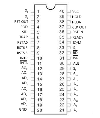
Power Supply and Clock Signals:
VCC +5 Volt power supply : pin 40
GND, ground : pin 20
X1 and X2, crystal network for frequency of internal clock : pin 1 and 2
CLK OUT, clock output as system clock for peripherals : pin 37
Address Bus:
A8 – A15 : pin 21 to 28
MSB of memory address.
Multiplexed Address or Data Bus:
AD0 – AD7 : pin 12 to 19
LSB of address and data
Control and Status Signal:
ALE, address latch enable : pin 30
RD’ : pin 32 and WR’ : pin 31
S0, S1 and IO/M’ : pin 29, 33 and 34
IO/M’ : high for I/O operation and low for memory operation
Interrupt and Externally Initiated Operation:
TRAP : pin 6
RST 7.5 to 5.5 : pin 7, 8, 9
INTR : pin 10
INTA’ : pin 11
HOLD, peripheral requesting bus : pin 39
HLDA, acknowledgement of hold request : pin 38
READY, delay microprocessor read/write cycle until peripheral is ready : pin 35
RESET IN’ : pin 36
RESET OUT : pin 3
Serial I/O Port:
SOD : pin 4
SID : pin 5
Pin Configuration of 8086
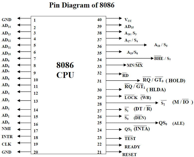
The pin configuration of 8086 Microprocessor is shown in the figure:
Timing Cycle
Machine Cycle
- A machine cycle is defined as the time required to complete one operation.
- It consists of: Op Code Fetch Cycle, Memory Read/Write Cycle and I/O Read/Write Cycle.
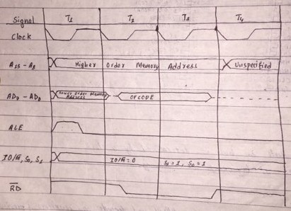
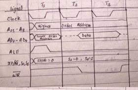
Op Code Fetch Cycle:
- Microprocessor fetches the machine code from memory register where it is stored.
- Fetch cycle is of 4 clock cycles as shown below:
- Microprocessor places 16-bit memory address from PC on address bus.
- At T1, high order address is placed at A8 – A15 and low order address at AD0 – AD7. ALE signal goes high. IO/M’ goes low and both S0 and S1 goes high.
- Control Unit sends control signal RD to enable memory chip and active during T2 and T3.
- The byte from memory location is placed on data bus into D0 – D7 and RD’ goes high.
- The instruction is decoded.
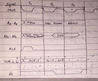
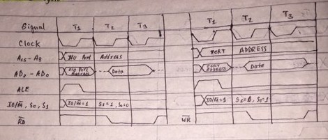
Memory Read Cycle:
For a read operation, once the output data are valid, the address input cannot be changed immediately to start another read operation. This is because the device needs a certain amount of time, called read recovery time, to complete its internal operations before the next memory operation. The sum of the access time and read recovery time is the memory read cycle time. This is the time needed between the start of a read operation and the start of the next memory cycle.
Memory Write Cycle:
The memory write cycle time can be similarly defined and may be different from the read cycle time. The Figure below illustrates the timing of a memory read cycle. The address is applied at point A, which is the beginning of the read cycle, and must be held stable during the entire cycle. In order to reduce the access time, the chip enable input should be applied before point B. The data output becomes valid after point C and remains valid as long as the address and chip enable inputs hold.
I/O Read and Write Cycle:
I/O instructions cause data read/write transfers which differ
from memory data transfers in the following ways:
1. The /IORQ (I/O Request) signal is asserted Low
instead of the /MREQ signal.
2. The 16-bit I/O address is not translated by the MMU.
3. A19-A16 are held Low.
4. A15-A8 may or may not be decoded by the I/O device.
At least one wait state (Tw) is always inserted for I/O
ready and write cycles (except Group 1 internal I/O
cycles)
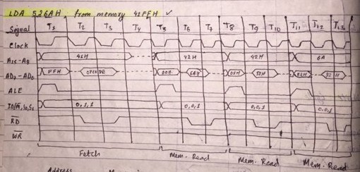
Q. Draw timing diagram or machine cycle for LDA 526A from memory 41FFH.
- Op Code Fetch
- Memory Read
- Memory Read
- Memory Read
Q. Draw timing diagram or machine cycle for STA 526AH.
- Op Code Fetch
- Memory Read (Lower Order Address)
- Memory Read (Higher Order Address)
- Memory Write
Q. Draw timing diagram or machine cycle for IN C0H.
- Op Code Fetch
- Memory Read
- I/O Read
Q. Draw timing diagram or machine cycle for OUT 01H.
- Op Code Fetch
- Memory Read
- I/O Write
Q. Draw timing diagram or machine cycle for MVI B, 43H.
- Op Code Fetch
- Memory Read
Q. Draw timing diagram or machine cycle for MOV C, A.
- Op Code Fetch
Q. Draw timing diagram or machine cycle for LXI B, 1652H.
- Op Code Fetch
-Memory Read (Lower)
- Memory Read (Upper)
Q. Draw timing diagram or machine cycle for INR M.
- Op Code Fetch
- Memory Read
- Memory Write
Q. Draw timing diagram or machine cycle for MOV M, A.
- Op Code Fetch
- Memory Write
Memory Device Hierarchy
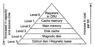
- Memory hierarchy is the pyramid of different memory technology that provides comparative analysis of memory technologies based on cost per bit, capacity, access time and so on.
- The main goal is to use the memory so as to obtain highest possible access speed minimizing the total cost.
- The memory hierarchy is shown below:
- As we go down, cost per bit decrease, capacity increase and access time increase.
Address Decoding
- Microprocessor is connected with memory and I/O device via a common address and data bus.
- Only one device can send data at a time.
- Address decoding is the technique that ensures that proper device gets addressed at proper time.
- The address of device is determined from the way in which address lines are used to derive selection signal or chip select.
Unique Address Decoding:
- All the address lines on the mapping mode are used for address decoding.
- It is expensive and complicated but fault proof.
Non-Unique Address Decoding:
- All the address lines are not used.
- It is cheaper and simple to design.
- It creates chance of address conflict.
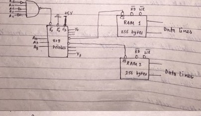
Q. Design address decoding circuit for 2 RAM of 256 bytes at 5300H.
256 bytes requires 8 address lines.
So, to address one of 256 bytes in each RAM requires 8 address lines A0 to A7.
Block Address A15 A14 A13 A12 A11 A10 A9 A8 A7 A6 A5 A4 A3 A2 A1 A0
1 Start 5300H 0 1 0 1 0 0 1 1 0 0 0 0 0 0 0 0
End 53FFH 0 1 0 1 0 0 1 1 1 1 1 1 1 1 1 1
2 Start 5400H 0 1 0 1 0 1 0 0 0 0 0 0 0 0 0 0
End 54FFH 0 1 0 1 0 1 0 0 1 1 1 1 1 1 1 1
Address Decoding Circuit:
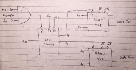
Q. Design decoding circuit to interface two 4 KB ROM at address 0000H.
4 KB = 4 * 1 KB = 4 * 2 ^ 10 = 2 ^ 12
So, to address one of 4KB in each ROM requires 12 address lines A0 to A11.
Block Address A15 A14 A13 A12 A11 A10 A9 A8 A7 A6 A5 A4 A3 A2 A1 A0
1 Start 0000H 0 0 0 0 0 0 0 0 0 0 0 0 0 0 0 0
End 0FFFH 0 0 0 0 1 1 1 1 1 1 1 1 1 1 1 1
2 Start 1000H 0 0 0 1 0 0 0 0 0 0 0 0 0 0 0 0
End 1FFFH 0 0 0 1 1 1 1 1 1 1 1 1 1 1 1 1
Address Decoding Circuit:
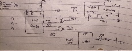
Q. Design a decoding circuit to interface i/p device with 8 switch and LED o/p device at 41H and 42H.
Block Address A7 A6 A5 A4 A3 A2 A1 A0
i/p port 41H 0 1 0 0 0 0 0 1
o/p port 42H 0 1 0 0 0 0 1 0
Address Decoding Circuit:
I/O Mapped and Memory Mapped I/O
I/O Mapped I/O:
- A device is identified with 8-bits address and operated by I/O related functions.
- IO/M’ is set i.e. 1
- At most 256 bytes can be identified uniquely.
- Low order address bits are used.
- It is used to map devices like 8255A, 8251A and so on.
Memory Mapped I/O:
- A device is identified with 16-bits address and enabled memory related functions.
- IO/M’ is reset i.e. 0
- CS signal is derived from 16-bits address line, thus total addressing capability is 64KB.
- It is used to map RAM, ROM and so on.
Serial Interface: Synchronous and Asynchronous Transmission
Synchronous and Asynchronous Bus
- A bus is said to be synchronous if occurrence of events on bus is determined by a clock.
- All events of synchronous bus start at the beginning of clock cycle.
- A bus is said to be asynchronous if occurrence of one event on bus follows and depends on occurrence of previous events.

Ⓒ Copyright ESign Technology 2019. A Product of ESign Technology. All Rights Reserved.