Memory Write Ability and Storage Permanence
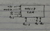
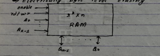
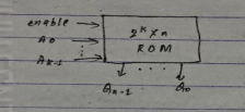
Memory Basics
- mxn memory stores m words of n bits each.
- m=2k where k = no of address input signals
- n indicates no of data signals
- r/w selects read or write
- enable : read or write only when asserted
Write Ability
Write ability is the manner and speed that a particular memory can be written . The ranges of write ability are:
1. High End (Processor writes to memory quickly – RAM )
2. Middle Range (Processor writes to memory slowly – FLASH , EEPROM )
3. Lower Range (Special equipment used to write to memory – EEPROM , OTP Rom)
4.Low End (bits stored only during fabrication – Masked ROM)
Storage Permanence
Storage permanence is the ability of memory to hold its stored bits after they have been weitten. The ranges are :-
1. High end (Never loss bits – Masked ROM )
2.Middle Range (holds bits for days or years after power cutoff – NVRAM )
3. Lower Range (holds bits as long as power is supplied – SRAM )
4. Lower End (lose bits immediately after written – DRAM )
Types of Memory
Random Access Memory (RAM)
- It can be read and written easily.
- It is volatile memory.
- Electrically byte level erasing
- Electrically write
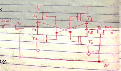
a) SRAM
1. Bits are stored as an on/off switches
2. Charges are not leaked
3. No refresh circuits
4. Larger per bit
5. Complex Instruction
6. Expensive
7. Faster
8. Cache
9. Use flip flops to store bit
10. In state 1:
C1 = high, C2 = Low
T2 T3 on
11. In state 0:
C1 = low C2= High
T2 T4 On
12. Write: apply value to B and B’
13. Read: Value is on B
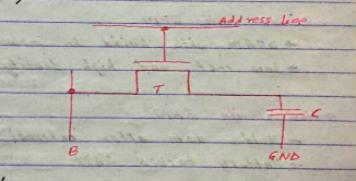
b) DRAM
1. Bits are stored as charge in capacitor.
2. Charges leak
3. Need refreshing
4. Have refresh circuits
5. Cheaper
6. Slower
7. Smaller per bit
8. Main memory
9. Level of charge determines value
- When address line is active, transistor switch closes,so bit is read or written.
- During write operation, transfer charge to capacitor,
- During read operation address line is selected and charge from capacitor is fed via B to sense amplifier.
c) Enhanced DRAM
-Enhanced DRAM are built around conventional DRAM core.
-It is a DRAM that includes small amount of static RAM so as to access memory faster.
-First,data is checked in SRAM.
-if miss , data is accessed from DRAM.
-Fast page mode DRAM : access row contents (RAS ,CAS,CAS,CAS)
-Extended data out DRAM: FPM with closely spaced CAS.
-Synchronous DRAM : Driven with rising clock edge.
-Double data rate SDRAM : SDRAM with both clock edges.
d) Pseudo Static RAM
-DRAM with built in memory refresh controller.
-Low cost and high density
e) NON Volatile RAM
-Holds data after external power removed.
-Battery backed RAM
-SRAM with EEPROM
Read only Memory (ROM)
- It can be read only.
- It is non-volatile memory.
Types of ROM
a) Masked ROM
-Programmed during fabrication by creating masks.
-Low write ability
-High storage performance
b) OTP ROM
-External equipment is needed to write
-Electrically write mechanism
c) EPROM
-Electrically write
-Erase usjng UV light (chip level)
d) EEPROM
-Byte level electrically erasing
-Electrical write
e) Flash Memory
-Block level electrically erasing
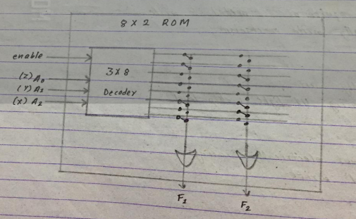
Composing Memory
Design 8 * 2 ROM:
| X | Y | Z | F1 | F2 |
|---|---|---|---|---|
| 0 | 0 | 0 | 1 | 0 |
| 0 | 0 | 1 | 1 | 0 |
| 0 | 1 | 0 | 0 | 1 |
| 0 | 1 | 1 | 0 | 1 |
| 1 | 0 | 0 | 0 | 0 |
| 1 | 0 | 1 | 1 | 1 |
| 1 | 1 | 0 | 0 | 1 |
| 1 | 1 | 1 | 1 | 0 |
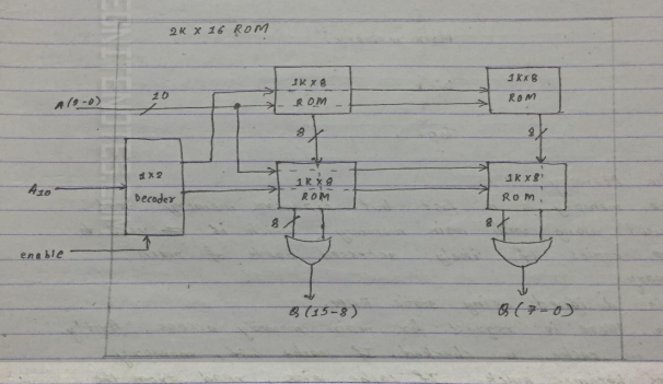
Compose 1K * 8 ROMs into 2K * 16 ROMs:
1K * 8
k = 10
n = 8
2K * 16
k = 11
n = 16
Memory Hierarchy and Cache
The general memory hierarchy is :
Processor --> Registers --> Cache --> Main Memory --> Disk --> Tape
Cache Memory
- Cache memory is a fast but expensive memory that is used along with main memory which is used to store copies of likely accessed parts of main memory.
- It is designed using static RAM,
- When there is request for main memory access,, firstly copy in cache is checked if cache hit, memory access becomes quick. If cache miss,read from main memory
Cache Mapping
1) Direct mapping
2) Fully associative mapping
3)Set associative mapping
Cache Replacement
1) Choosing which cache block to replace
2)Random replacement
3)Least recently used (LRU) policy
4)First in first out (FIFO) policy
Cache write techniques
-Updating the main memory
-Write Through (Write to main memory whenever cache is written)
-Write back (write to main memory when cache block is being replaced)

Ⓒ Copyright ESign Technology 2019. A Product of ESign Technology. All Rights Reserved.