Microprocessor Based System
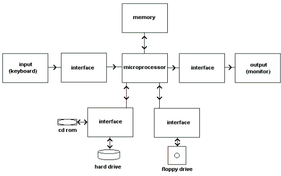
Microprocessor based system includes microprocessor, input/output and memory organized around a common path called bus as shown in given figure:
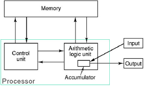
Microprocessor-
- Microprocessor is a programmable, clock driven register based device that reads binary instruction from memory, accepts binary data as input, process data according to instruction and provide result in output.
- ALU is responsible to perform arithmetic and logical operations on data.
- Registers are used to store data temporarily during program execution.
- Control unit provides necessary timing and control signals to all the operations controlling flow of data between microprocessor and other components.
Memory
- Memory stores binary information i.e. instruction and data.
- Microprocessor reads instruction and data from memory.
- Results can be stored in memory for later use.
- ROM stores programs that do not need alterations.
- RAM stores user programs and data that can be altered.
Input/Output
- Input devices transfer binary information from outside world to microprocessor.
- Output devices transfer data from microprocessor to outside world.
System Bus
- System bus is the communication path between microprocessor and peripherals.
Bus Organization and its Types
- Bus is a common channel through which bits are transferred from source to destination.
- Common bus system provides common lines for each bit of register.
- Control signals determine the selection of register for each transfer.
Types of Bus
1. Data Bus
Data lines provides a path for transferring data.
Such lines are called data bus.
2. Address Bus
Address lines determine the source and destination of data on data bus.
Such lines are called address bus.
3. Control Bus
Control lines control the access to and the use of data and address bus.
Such lines are called control bus.
It transmits timing and control signals for each operation.
Automated Calculator
- Data processing device carrying out arithmetic and logical operations is called automated calculator.
The major features of automated calculator are as follows:
a) Easy interface with keyboard and displays.
b) Able to handle decimal digits.
c) Able to execute programs stored in ROM.
d) Extended for execution of many mathematical functions.
e) Flexible to use in many areas with same design.
f) Low cost, small in size and low power consumption.
Stored Program Concept and Von Neumann Machine
Von-Neumann Machine
- Shared program concept is the concept of storing instructions in memory alongside the data so that the system can get instructions from memory and programs can be altered by setting values of a portion of memory.
- Adopted in Von-Neumann Machine.
- Main memory is used to store both data and instructions.
- Fundamental basis for modern computer architecture.
- A single bus is used.
- It has limited processing speed.
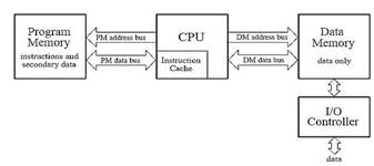
Harvard Architecture
- Uses separate memory space for instructions and data.
- Instructions and data can be fetched concurrently.
- Improvement in processing speed.
- Two data bus and two address bus are used.
Processing Cycle of a Stored Program Computer
1. Fetch
- CPU sends PC to MAR and sends READ command to control bus. In response to read command, the memory returns data stored at memory location indicated by PC on data bus. The CPU copies data from data bus to MBR. After some time, data from MBR is copied to IR. The PC is incremented so that it points to next instruction in memory. The CU fetches instruction’s address from memory.
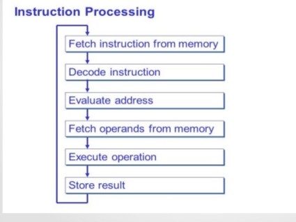
2. Decode
- It allows CPU to determine what instruction is to be performed and tell how many operands are needed to be fetched.
- The processing of decoding instruction is done by the Control Unit.
3. Fetch Data
- In this step, the required data for executing an instruction are fetched from their respective registers and addresses.
4. Execute
- The actual function of the instruction is performed in this step.
- ALU is responsible for arithmetic and logical functions.
5. Write Back
- The results generated by execution cycle is stored in main memory or sent to output device.
Hardwired vs Microprogrammed Control Unit
Hardwired CU:
It is a combinational circuit which cannot be programmed.
Boolean expression for each control signal should be derived as a function of input.
It is difficult to design.
It has faster mode of operation.
The design has to be modified if rewriting is needed.
Micro-Programmed CU:
Control information is stored in memory which can be programmed.
It is cheaper and simple to design.
It has slow mode of operation.
The same design can be used for multiple purposes.
Introduction to Register Transfer Language
RTL is the systematic notation used to describe the main operation transfer among registers.
RTL for MOV A, B:
Fetch Cycle:
T1: MAR <- PC
T2: MBR <- [MAR]
T3: IR <- MBR
PC <- PC + 1
Execute Cycle:
T4: MAR <- (IR ( ADDRESS OF B ))
T5: MAR <- [B]
T6: MAR <- (IR ( ADDRESS OF A ))
T7: A <- MAR
RTL for MVI A, 02H:
Fetch Cycle:
T1: MAR <- PC
T2: MBR <- [MAR]
T3: IR <- MBR
PC <- PC + 1
Execute Cycle:
T4: MBR <- (IR ( ADDRESS OF IMMEDIATE DATA ))
T5: MAR <- (IR ( ADDRESS OF A ))
T6: [MAR] <- MBR
RTL for LXI D, 9050H:
Fetch Cycle:
T1: MAR <- PC
T2: MBR <- [MAR]
T3: IR <- MBR
PC <- PC + 1
Execute Cycle:
T4: MBR <- IR [Address of immediate data (LSB)]
T5: MAR <- IR [Address of E]
T6: E <- MBR
T7: MBR <- IR [Address of immediate data (MSB)]
T8: MAR <- IR [Address of D]
T6: D <- MBR
- by SURAJ AWAL

Ⓒ Copyright ESign Technology 2019. A Product of ESign Technology. All Rights Reserved.