Full Custom IC Technology
-All layers are optimized for a particular ES implementation
-It involves placement of transistors to minimize interconnection length ,sizing transistor to optimize signal transmission and routing wires among transistors.
-It has high NRE cost and long time to market .
-It provides excellent performance ,small size and power.
Semi Custom IC Technology
- The lower layers are fully build leaving the upper layers.
- It has low NRE and less time to market.
- It needs to integrate with full custom IC for critical regions of design.
PLD IC Technology
- All layers already exists with a programmable circuit.
- It involves creation or destruction of connection between wires that connect gates,
- It has very low NRE and instant time-to-market.
- EPGA is a complex pld that offers general connectivity among blacks of logic.
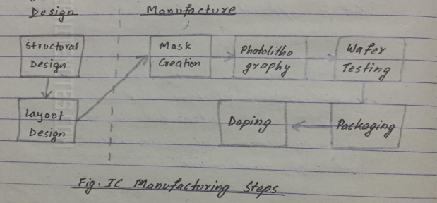
Steps in IC Manufacturing
IC Manufacturing:
IC is a semiconductor wafer in which various active and passive components along with external connections are fabricated in extremely tiny silicon chips.The various steps for IC manufacturing are as follows:
1. Wafer Production
2. Photolithography
3. Doping
4.Metallization
5.Assembly and packaging
Wafer Production
Wafer is a round slice of semiconductor material such as silicon. In IC , silicon wafer is used :
- Purified polycrystalline SI is created from sand.
- It is heated to produce molten liquid.
- A small piece of solid Si is dipped into molten liquid.
- Solid silicon is slowly pulled from the melt.
- The liquid cools to form single crystal.
- A thin round wafer is cut using wafer slicer.
- The wafer surface is smoothened by polishing.
- It is cleaned and dried using high purity low particle chemicals
Photolithography
- Photolithography is the process of printing a pattern of mask into the silicon wafer. It is carried out using light sensitive photoresist and controlled exposure to light.
- Positive photolithography prints a pattern that is same as the pattern on the mask.
- Negative photolithography prints a pattern that is opposite of the pattern as that on the mask.
Doping
- To alter the electrical character of silicon ,atom with one less electron and atom with one more electron are introduced in to the area.
- The impurity atoms in semiconductor materials are moved at high temperature .
Metallization
- It is used to create contact with Si and to make interconnections on chip.
- A thin layer of aluminium is deposited over the wafer.
Assembly and packaging
Each wafer consists of many chips. These chips are separated and packaged by scribing and cleaving. A diamond saw is used to cut wafer into chips. The tested and verified chip is mounted into a package. It is encapsulated for protection.
Water condition before
-Surface includes film composition , bare surface and reflectivity.
-It affects
-photoresist to wafer adhesion
-alignment accuracy
-Linewidth resolution
-exposure settings
-bake time.
Wafer condition after
-Resist coated wafer.
-patterned resist layer
-withstand etching
-withstand ion implanting
Photolithography Steps in Detail:
1. Surface preparation
- It increases adhesion of photoresist material to the substrate
- Dehydration bake removes water from substrate by baking at temp of 200 degree Celsius to 400 degree Celsius for 30 to 60 minutes.
- The substrate is then cooled and coated.
- Adhesion promoters like hexamethyl disilizane are used to react chemically with surface and replace –OH with organic function group.
2.Photoresist coating
- A thin uniform coating of photoresist is accomplished by spin coating
- The photoresist in liquid form is poured into the wafer and then spun at a high speed to produce desired film
- thickness is affected by spin speed , time and volume of resist.
3. Soft Bake
- The film contain about 20-40% by weight solvent.
- It involves drying or removing of excess solvent.
- it helps to stabilize the resist film.
- it improves adhesion and uniformity.
- It is baked in oven at 95 deg Celsius for 35 minutes.
4.Alignment and exposure
- A photo mask with pattern on one side is aligned over the wafer.
- A uv light (12mw) is exposed to the surface.
- The exposure time affects critical dimension. With increase in expose time, F increase.
5. Develop
- Soluble areas of photoresist are dissolved by developer chemical .
- A visible patterns appear on wafer.
6.Hard bake
- It hardens the final resist image.
- Hard bake is done at temp of 110 deg Celsius for about 30 minutes.
- It improves adhesion.
7.Develop Inspection
- The resist patterned wafer is inspected for particles,defects,CD, linewidth resolution and overlay accuracy.
8. Etching
- It is the selective removal of upper layer of wafer.
- It is performed either by using wet chemicals or in a dry plasma environment.
9. Strip
- It is the process of removing photo resist.
- Wet acid strip or dry plasma strip.
10. Final inspection
- Complete removal of photoresist.
- Pattern on wafer to ne correct .
- Defects, particles,, step height and CD are checked.
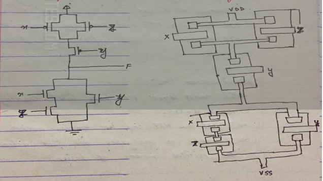
Show top down view of circuit: F = xz + y on an IC.
The diagram is shown below:
Ⓒ Copyright ESign Technology 2019. A Product of ESign Technology. All Rights Reserved.